Developing Unconventional Solutions for Conventional Problems
We work directly with clients to develop a customized solution that meets their precise needs. We can offer our customers any and all of the following services:
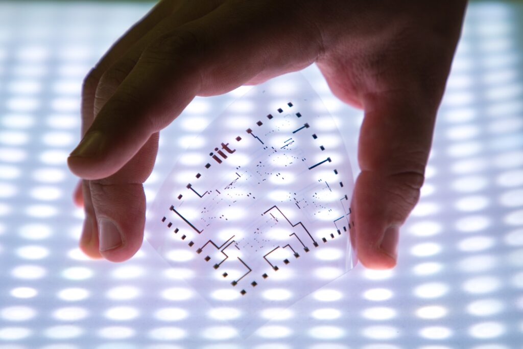
Customize Intrinsiq ink to their application
Determine the appropriate printing conditions for the client’s chosen deposition method (i.e. drop velocity for inkjet) enabling the use of commercially available systems
Work with printing equipment manufacturers to validate our ink in their system
Work with sintering equipment manufacturers to determine the sintering conditions and operational boundaries for broadband flash systems
Develop the laser sintering conditions where applicable
Provide lab scale systems for laser sintering
Co-develop all associated processes
Copper Applications
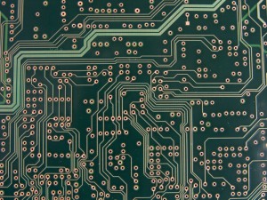
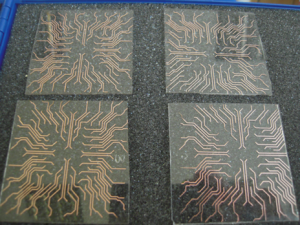
PCB & Interconnect Metallization
Intrinsiq’ s inkjettable and screen printable copper pastes are used to metallize vias and boards. Our additive process reduces copper consumption, reduces the use of harmful etchants and provides excellent results. Light sintering also reduces the requirement of heat tolerance of the substrate and opens the door to less expensive and flexible solutions.
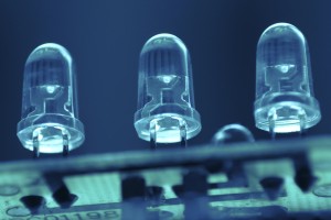
LED Metallization
Intrinsiq inks provide not only the metallization of circuit boards but can provide metallization directly into the LED. As an excellent thermal conductor, printed copper can increase the lifetime while providing good conductivity.
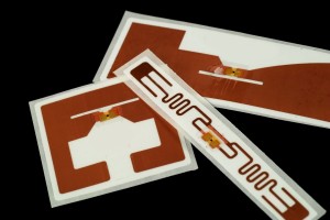
Antennas
Intrinsiq inks provide a cost-effective direct printing solution for antennas for RFID and mobile applications. By directly printing and sintering on heat sensitive media such as packaging and paper, copper antennas are considerably less expensive in this most cost-sensitive market.
Seed Layers
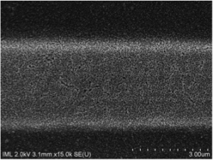
Intrinsiq prints narrow line width copper lines for seed layers for use in conjunction with electroless chemistry.
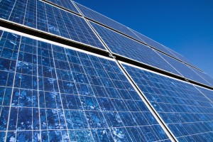
Metallization for Solar cells
Intrinsiq is developing copper paste specifically for use with thin film photovoltaic solar cells. This program seeks to reduce the cost of metallization by replacing expensive silver paste with cost effective copper.
Touch Screens
Inrinsiq’s unique ink and process allows the printing of conductive tracks of less than 5 micrometers on ITO coated glass. View the video of busbar fabrication through youtube, link located at top right.
Developmental Programs
NiSi Contacts for PV
Airhandleable, printable NiSi is well suited for printing on ARC layers in Si solar cells. This dopable contact technology is of use in many applications where contacts are printed on Si substrates.
Copper for Underfills and Packaging
The ability to control the size of particles, combined with the thermally conductive nature of copper make it highly suitable for spacers and underfiill technology. In a time where size is often limited by thermal load, Intrinsiq is developing materials suitable for thermal management in packaging.
Doped Silicon Ink for Logic Applications
Intrinsiq Materials has developed n and p dope silicon ink. Si ink can be deposited in air and has demonstrated mobilities equal to that of amorphous silicon.
For More Information And New Features Subscribe Our Newsletter